
🛠️ Hardware Engineering & Schematics
The IntelliKeep system encompasses two custom printed circuit board assemblies: the ultra-compact, coin-cell-powered BLE Asset Tag and the mains-powered ESP32-S3 Base Station Hub. Both were authored in KiCad, fabricated as multi-layer FR4 PCBs, and packaged inside custom 3D-printed enclosures designed in Autodesk Fusion 360.
1. BLE Tag Hardware Architecture
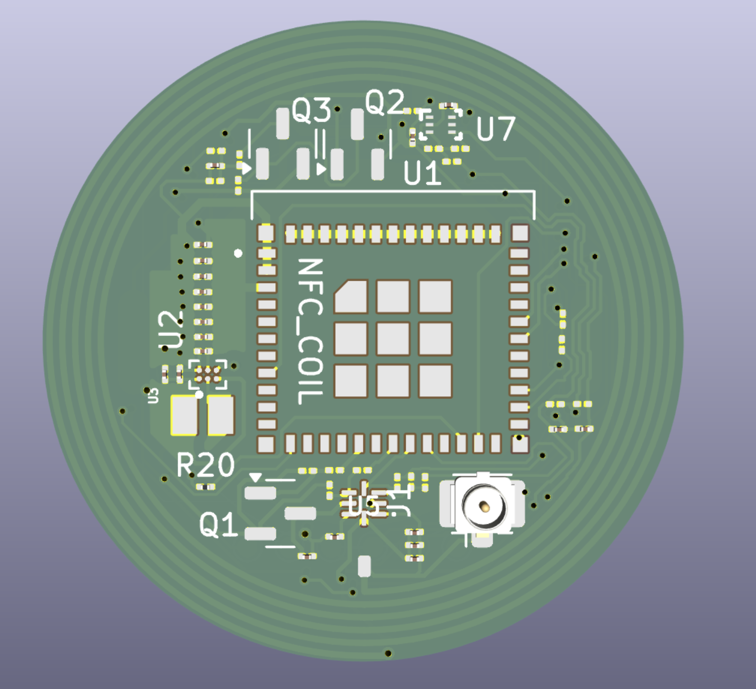
The BLE tag is the most resource-constrained hardware in the IntelliKeep ecosystem. To attach discreetly to equipment and tools, it must maintain a miniature form factor, minimize sleep current into the low nanoamp range, wake in milliseconds to transmit BLE packets, monitor for enclosure tampering without continuous MCU polling, and allow smartphone NFC onboarding.
Key Component Selection:
- Microcontroller: Espressif
ESP32-C3-MINI-1U-N4. Chosen for its compact footprint, RISC-V 32-bit core, integrated 4MB SPI flash, certified 2.4 GHz RF front end, and versatile deep-sleep RTC wakeup modes. - RF Interface: U.FL coaxial connector routed directly to an external 2.45 GHz antenna, minimizing parasitic detuning on a dense mixed-signal PCB.
- Coin-Cell Retainer: Linx
BAT-HLD-002-SMTsurface-mount battery holder accommodating CR2032 or rechargeable LIR2032 coin cells.
Tag Subsystem Circuit Analysis
A. Ultra-Low Iq Boost Regulator (TPS610994)
A standard CR2032 coin cell drops in terminal voltage from 3.0V down to ~2.0V as it depletes, which falls below the stable operating voltage of the ESP32-C3 (3.0V–3.6V). The tag uses the Texas Instruments TPS610994YFFR synchronous boost converter in a miniature DSBGA package, paired with a high-saturation 4.7 µH inductor.
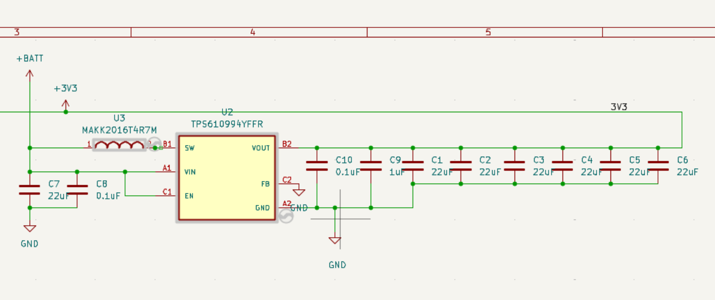
The TPS610994 draws an ultra-low quiescent current of only 1 µA during sleep, but the ESP32-C3 requires momentary current pulses up to 150–200 mA when enabling the RF synthesizer and transmitting BLE packets. Low-ESR ceramic output capacitors buffer this transient load, preventing voltage rail collapse during radio bursts.
B. Nanopower Optical Tamper Detection
Continuous firmware sampling of an ambient light sensor would consume tens of microamps, depleting a coin cell in weeks. IntelliKeep moves the tamper decision entirely into ultra-low-power analog hardware using a Vishay VBPW34S PIN photodiode and a Texas Instruments TLV3691IDPFR nanopower comparator.
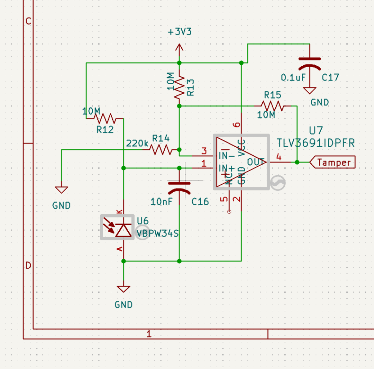
The comparator draws less than 75 nA of quiescent current. While the tag remains sealed within its dark enclosure, the photodiode stays non-conductive and the comparator output remains low. If an unauthorized person removes the enclosure lid or detaches the tag, incoming photons immediately trigger the comparator output high, firing an asynchronous hardware interrupt to wake the ESP32-C3 and transmit an immediate tamper alarm (Reason Code 1).
C. Switched Battery Measurement Divider
Measuring a battery voltage using a direct resistive voltage divider connected to an ADC pin creates a permanent leakage current path from VCC to GND. For a 2MΩ divider, this would leak 1.5 µA permanently—exceeding the entire deep-sleep budget of the system!
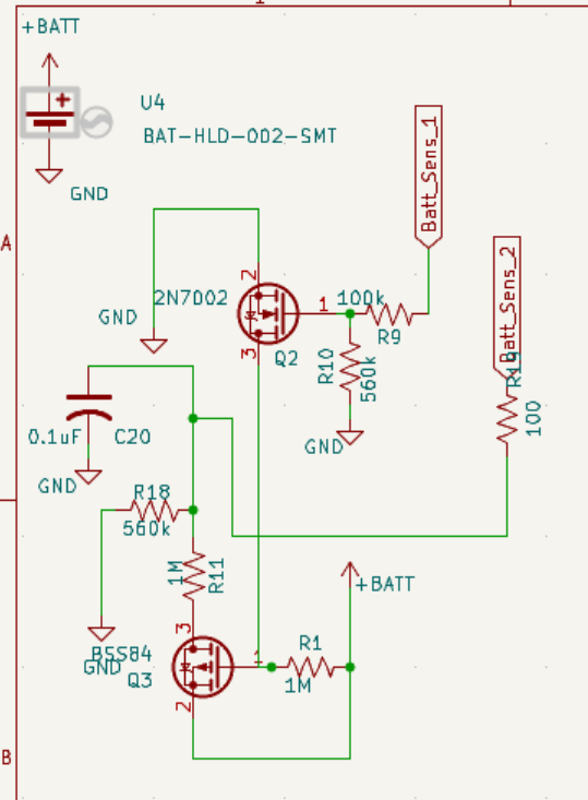
IntelliKeep isolates the divider using a high-side BSS84 P-channel MOSFET driven by a low-side 2N7002 N-channel MOSFET. When the MCU is sleeping, the divider is completely disconnected (0 nA leakage). During wake, GPIO assertions briefly switch on the PMOS, sample the ADC, and immediately disconnect the path.
D. 13.56 MHz Planar Spiral NFC Subsystem
Tag enrollment is expedited via an NXP NT3H2111W0FHKH NFC tag IC. Rather than purchasing bulky discrete NFC stickers, a custom 5-turn planar PCB spiral coil with an outer diameter of ~30 mm was routed directly onto the outer copper layers.
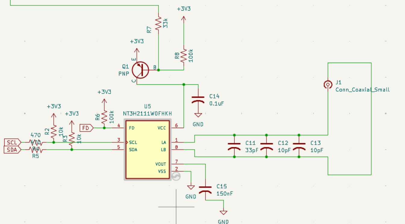
Using an RF Vector Network Analyzer (VNA), the coil inductance was measured at ~0.5 µH. When combined with the NT3H input capacitance (50 pF) and PCB trace parasitics, the tank resonance was tuned precisely to 13.56 MHz, yielding reliable smartphone NDEF reads and writes at distances up to 2 cm.
Tag Mechanical Packaging (Autodesk Fusion 360)
The asset tag is enclosed in a miniature cylindrical housing measuring 33 mm in diameter and 11.5 mm thick. It uses a snap-together friction-fit rim requiring no metal screws or fasteners, minimizing manufacturing cost and assembly time.
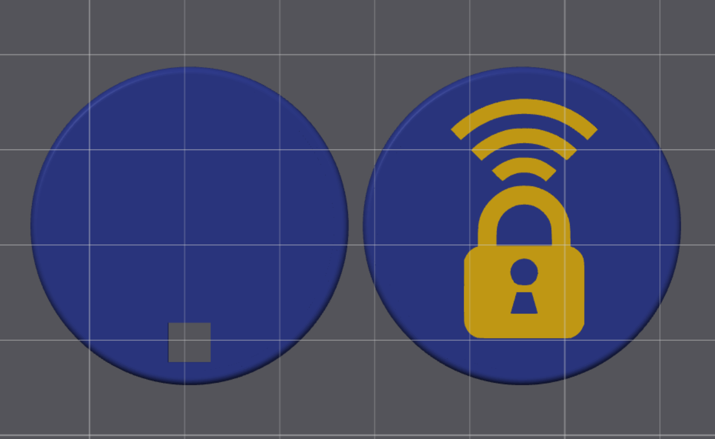
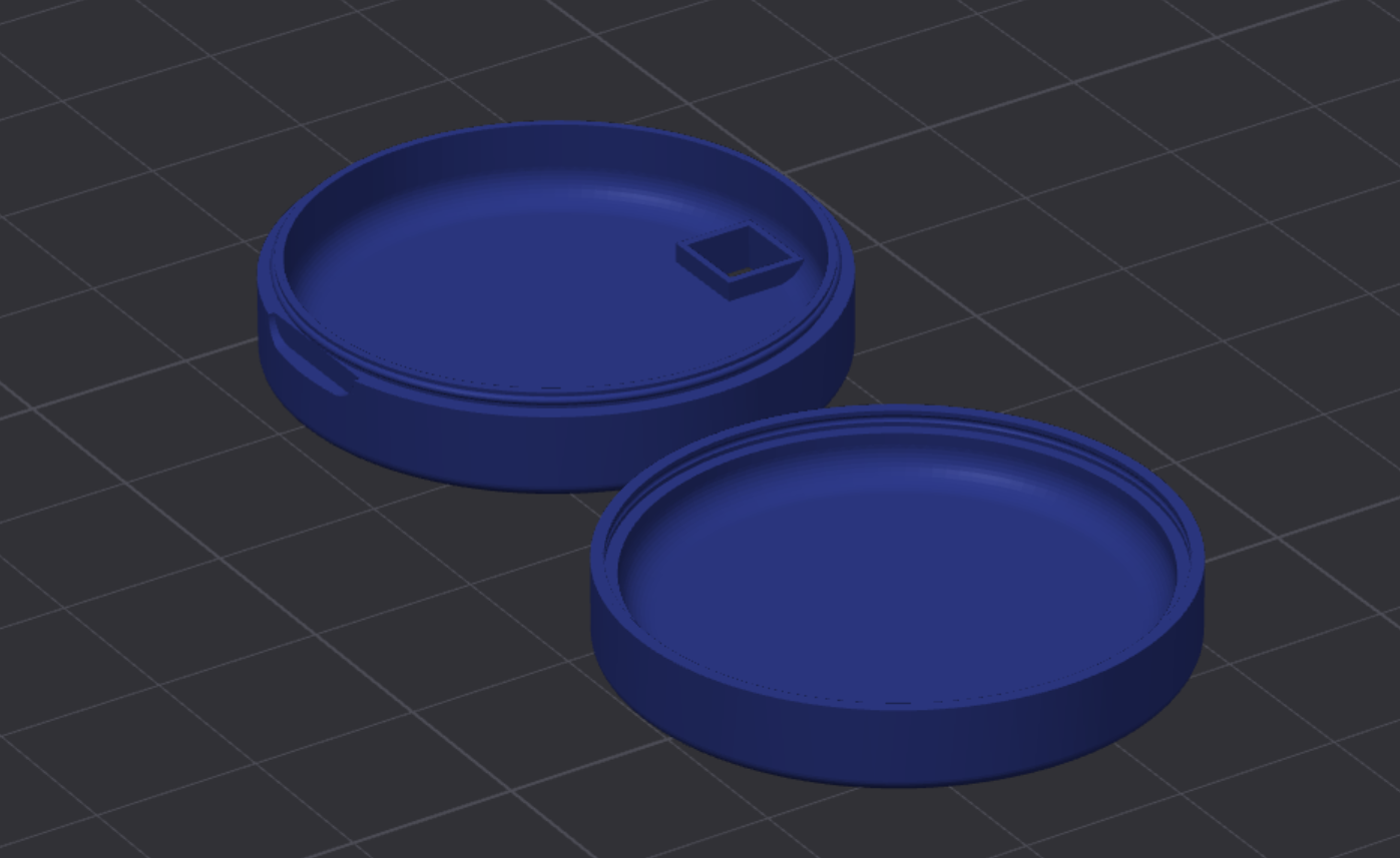
The enclosure incorporates a recessed optical window directly above the VBPW34S photodiode. When mounted against an asset, the surface completely blocks ambient light; prying the tag away allows ambient light to strike the photodiode, triggering the alarm instantaneously.
2. Base Station Hardware Architecture
The base station operates as an always-on mains-powered gateway. It prioritizes continuous radio reception, multi-protocol bridging, and high-performance processing over power reduction:
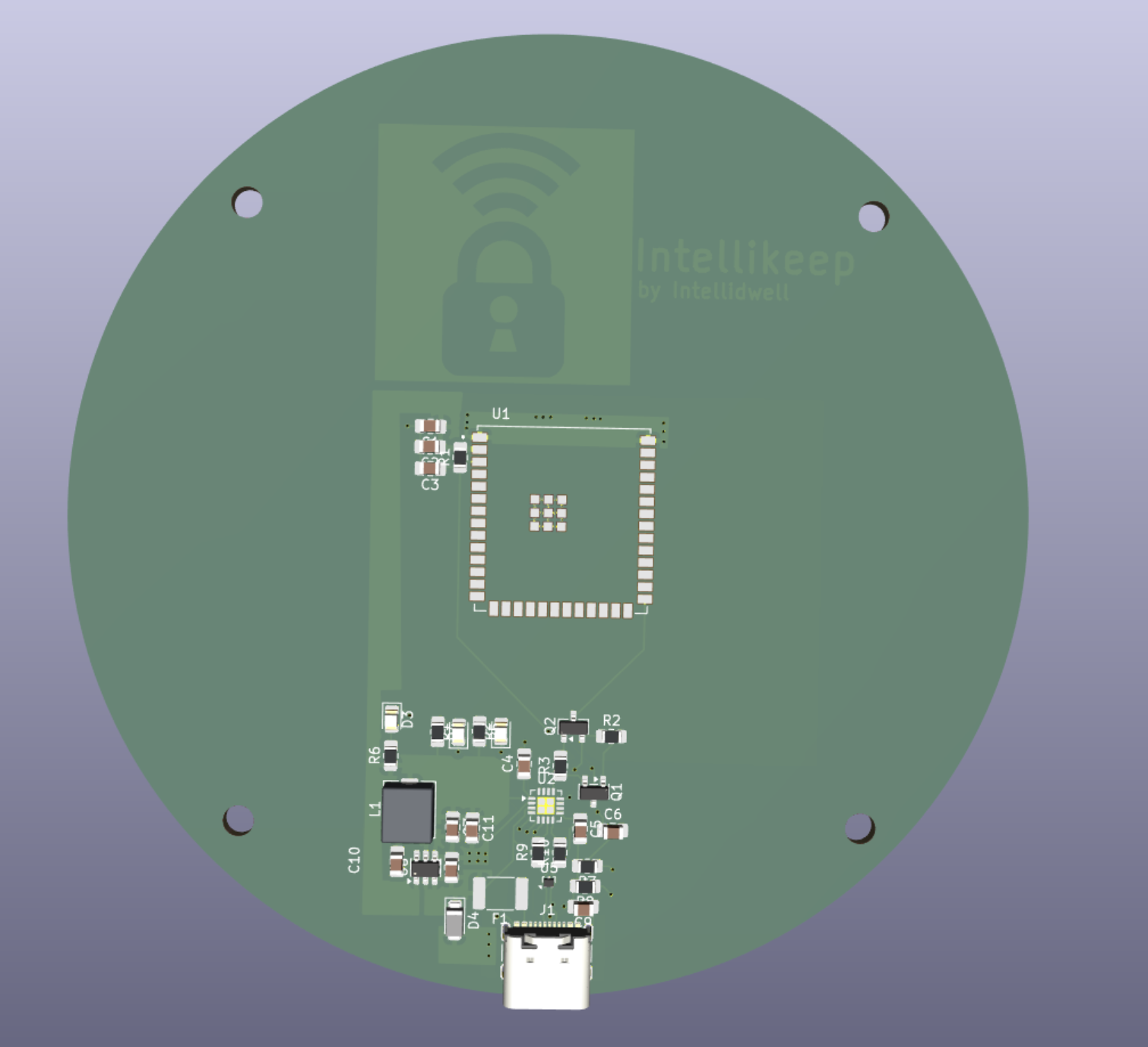
Key Components:
- Processing Core: Espressif
ESP32-S3-WROOM-1U-N16featuring dual Xtensa 32-bit LX7 cores at 240 MHz, 16MB SPI flash, 512KB SRAM, and Wi-Fi 802.11 b/g/n + Bluetooth 5 (LE) mesh radio. - Power Input: GCT
USB4105USB Type-C receptacle with ESD clamp diodes, TVS surge protection, and a resettable polyfuse. - Main Buck Regulator: Diodes Inc
AP63203WUsynchronous buck converter delivering a steady 3.3V rail at up to 2A with high thermal efficiency. - Serial Flashing Bridge: WCH
CH343PUSB-to-UART bridge allowing 1-click firmware upload and real-time serial diagnostics over the native USB-C port.
Base Station Mechanical Enclosure
The base station enclosure follows the same cylindrical aesthetic as the tag, measuring 105 mm in diameter and 85 mm tall:
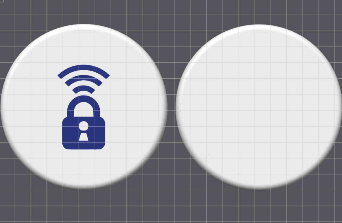
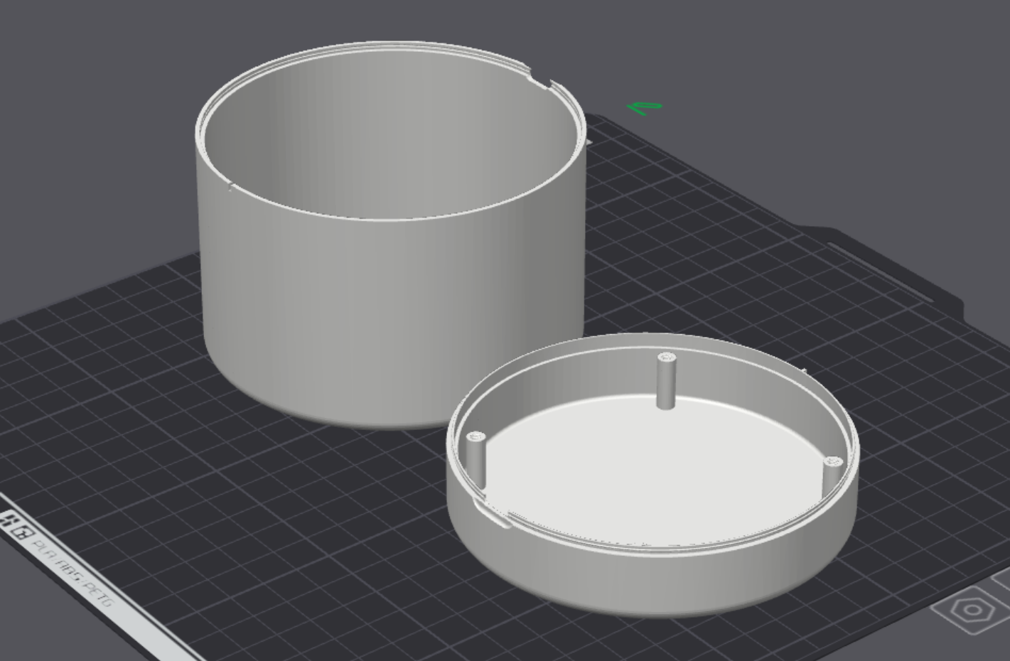
The enclosure lid incorporates a press-fit retention collar that secures the internal 2.4 GHz antenna vertically in the center of the cylinder, maximizing omnidirectional RF reception across the property without external protruding antennas.
Estimated Bill of Materials (BOM) Costs
Cost modeling was conducted across multiple manufacturing quantity tiers to demonstrate commercial feasibility for property operators and small businesses:
BLE Asset Tag BOM Cost
| Item / Description | Qty 1 | Qty 10 | Qty 100 |
|---|---|---|---|
| Tag Electronics (ESP32-C3, TPS610994, NT3H2111, Passives) | $11.00 | $7.81 | $6.45 |
| 4-Layer Custom PCB (FR4, ENIG finish) | $2.50 | $1.00 | $0.75 |
| Battery (CR2032 / LIR2032 Coin Cell) | $0.60 | $0.60 | $0.60 |
| Antenna (2.45 GHz U.FL Coaxial) | $1.90 | $1.90 | $1.90 |
| 3D Printed Enclosure (PLA / PETG) | $0.10 | $0.10 | $0.10 |
| Estimated Total Per Tag | $16.10 | $11.41 | $9.80 |
Base Station Hub BOM Cost
| Item / Description | Qty 1 | Qty 10 | Qty 100 |
|---|---|---|---|
| Base Station PCB (2-Layer FR4) | $6.00 | $4.50 | $2.00 |
| Components (ESP32-S3-WROOM-1U, AP63203, CH343P, Passives) | $15.60 | $10.72 | $8.74 |
| 3D Printed Cylindrical Enclosure | $3.75 | $3.75 | $3.75 |
| Antenna (Internal 2.4 GHz Dipole) | $3.50 | $3.50 | $3.50 |
| Estimated Total Per Base Station | $28.85 | $22.47 | $17.99 |